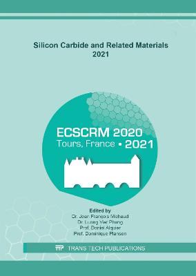
Silicon Carbide and Related Materials 2021
 portes grátis
Silicon Carbide and Related Materials 2021
Michaud, Jean Francois; Alquier, Daniel; Phung, Luong Viet; Planson, Dominique
Trans Tech Publications Ltd
06/2022
728
Mole
Inglês
9783035727609
15 a 20 dias
1350
Descrição não disponível.
Preface
Chapter 1: Material Growth and Wafer Manufacturing
Models for Impurity Incorporation during Vapor-Phase Epitaxy
Liquid Si-Induced 4H-SiC Surface Structuring Using a Sandwich Configuration
Defect Reduction in Epilayers for SiC Trench MOSFETs by Enhanced Epitaxial Growth
High Temperature Etching for Threading Dislocation Investigation on GaN Epi-Layer
3C-SiC Heteroepitaxial Layers Grown on Silicon Substrates with Various Orientations
A Novel Approach of Utilizing Mechanically Flexible SiC Substrate to Grow Crack-Free AlN Bulk Crystal by Thermal Strain Relaxation Functionality
The Impact of Defect Density on Mechanical Characteristics of 4H-SiC Substrates
Aluminum Activation in 4H-SiC Measured on Laterally Contacted MOS Capacitors with a Buried Current-Spreading Layer
Silicon Carbide Formation in Reactive Silicon-Carbon Multilayers
Impact of Epitaxial Defects on Device Behavior and their Correlation to the Reverse Characteristics of SiC Devices
Advances in 200 mm 4H SiC Wafer Development and Production
Toward the Reproducible Growth of Graphene on Wide SiC Steps: A Study of the Geometric Properties of 4H-SiC (0001) Substrates
Effect of N and Al Doping on 3C-SiC Stacking Faults
Impact of N Doping on 3C-SiC Defects
Large Area Growth of Cubic Silicon Carbide Using Close Space PVT by Application of Homoepitaxial Seeding
In Situ Monitoring of Unintentionally Released Nitrogen Gas in the Initial PVT Silicon Carbide Growth Process Using Mass Spectrometry
Precise Control of Al Incorporation during CVD Growth of SiC Epilayers by Using Hydrogen Chloride
Analysis of the Morphology of the Growth Interface as a Function of the Gas Phase Composition during the PVT Growth of Silicon Carbide
Designing SiC Based CMUT Structures: An Original Approach and Related Material Issues
Interfacial Dislocation Reduction by Optimizing Process Condition in SiC Epitaxy
Review of Sublimation Growth of SiC Bulk Crystals
Applicability of a Flat-Bed Birefringence Setup for the Determination of Threading Dislocations of Silicon Carbide Wafers
Chemical Vapor Deposition of 3C-SiC on [100] Oriented Silicon at Low Temperature < 1200 degreesC for Photonic Applications
SiC Mass Commercialization: Present Status and Barriers to Overcome
150 mm SiC Engineered Substrates for High-Voltage Power Devices
Impact of Surface Emissivity on Crystal Growth and Epitaxial Deposition
Vanadium Incorporation in 3C-SiC Epilayers and its Consequences for Electrical Properties of 3C-SiC Material
Opening through 200 mm Silicon Carbide Epitaxy
Chapter 2: Processing
Novel Vitrified-Bond Ultra-Fine Grinding Technology for SiC Polishing
Charge Trapping Mechanisms in Nitridated SiO2/ 4H-SiC MOSFET Interfaces: Threshold Voltage Instability and Interface Chemistry
Impact of Dislocation on Warpage of Thinned 4H-SiC Wafers
Silicon Carbide - Graphene Nano-Gratings on 4H and 6H Semi-Insulating SiC
Polish Scratch Simulation vs. Polish Tool Type
Study of Laser Backside Ohmic Contact Formation of SiC-Ni Interface to Evaluate the Process Influence on the Electrical Characteristics
Via Size-Dependent Properties of TiAl Ohmic Contacts on 4H-SiC
Engineering the Schottky Interface of 3.3 kV SiC JBS Diodes Using a P2O5 Surface Passivation Treatment
The Development of Monolithic Silicon Carbide Intracortical Neural Interfaces for Long-Term Human Implantation
Graphite Assisted P and Al Implanted 4H-SiC Laser Annealing
A Novel Tool Layout and Process for Single Side Wet Electrochemical Processing of Porous Silicon Carbide Layers without Edge Exclusion
Multiscale Simulations of Plasma Etching in Silicon Carbide Structures
Optimisation of Ti Ohmic Contacts Formed by Laser Annealing on 4H-SiC
Ohmic Contact Formation on 4H-SiC with a Low Thermal Budget by Means of Shallow Phosphorous Ion Implantation
Highest Quality and Repeatability for Single Wafer 150mm SiC CMP Designed for High Volume Manufacturing
Mechanism Governing Surface Roughening of Al Ion Implanted 4H-SiC during Annealing under a C-Cap
Estimation of Activation and Compensation Ratios in Al+ Ion Implanted 4H-SiC: Comparison of Two Methodologies
Decoration and Density Increase of Dislocations in PVT-Grown SiC Boules with Post-Growth Thermal Processing
Chapter 3: Characterization, Modelling and Defect Engineering
Identification of High Resolution Transient Thermal Network Model for Power Module Packages
Transmission Electron Microscopy Study of Single Shockley Stacking Faults in 4H-SiC Expanded from Basal Plane Dislocation Segments Accompanied by Threading Edge Dislocations on both Ends
Phosphorous and Aluminum Implantation for MOSFET Manufacturing: Revisiting Implantation Dose Rate and Subsequent Surface Morphology
Evaluation of Defects in a SiC Substrate Using the Photoluminescence Measurement Method
Effective Method (Selective E-V-C Technique) to Screen out the BPDs that Cause Reliability Degradation
Optical Characterization of 4H-SiC Thick Epitaxial Layer for Particle Detection
Automatic Image Analysis of Stackingfault
Observation of Fast Near-Interface Traps in 4H-SiC MOS Capacitors Using Capacitance Voltage Analysis at Cryogenic Temperatures
Enhanced Resonant Raman Scattering of GaN Functional Layers Using Al Thin Films - A Versatile Tool for Multilayer Structure Analysis
Microscopic Evaluation of Al2O3/p-Type Diamond (111) Interfaces Using Scanning Nonlinear Dielectric Microscopy
Measurement of Dislocation Density in SiC Wafers Using Production XRT
Computational Study of the Silicon Vacancy in 3C-SiC and Perspectives for Quantum Technologies
Depth-Resolved Study of the SiO2- SiC Interface Using Low-Energy Muon Spin Rotation Spectroscopy
Residual Stress Measurement by Raman on Surface-Micromachined Monocrystalline 3C-SiC on Silicon on insulator
The Improved Reliability Performance of Post-Deposition Annealed ALD-SiO2
KPFM - Raman Spectroscopy Coupled Technique for the Characterization of Wide Bandgap Semiconductor Devices
Surface Potential Fluctuations of SiO2/SiC Interfaces Investigated by Local Capacitance-Voltage Profiling Based on Time-Resolved Scanning Nonlinear Dielectric Microscopy
4H-SiC PiN Diode Protected by Narrow Field Rings Investigated by the Micro-OBIC Method
Sensitivity of Dit Extraction at the SiO2/SiC Interface Using Quasi-Static Capacitance-Voltage Measurements
Synchrotron X-Ray Topography Characterization of Power Electronic GaN Materials
Dislocation Contrast Analysis in Weak Beam Synchrotron X-Ray Topography
Investigation of Lattice Strain in High Energy Implanted 4H-SiC Wafers by Al or N Atoms
Ray-Tracing Simulation Analysis of Effective Penetration Depths on Grazing Incidence Synchrotron X-Ray Topographic Images of Basal Plane Dislocations in 4H-SiC Wafers
Stability, Evolution and Diffusion of Intrinsic Point Defects in 4H-SiC
Nitrogen Investigation by SIMS in Two Wide Band-Gap Semiconductors: Diamond and Silicon Carbide
Latest Advances in the Implementation and Characterization of High-K Gate Dielectrics in SiC Power MOSFETs
Fast Defect Mapping at the SiO2/ SiC Interface Using Confocal Photoluminescence
Evaluation of Line-Shape Defect in Epitaxial Wafer
Electrical Scanning Probe Microscopy Investigation of Schottky and Metal-Oxide Junctions on Hetero-Epitaxial 3C-Si? on Silicon
A Deeper Look into the Effects of Extended Defects in SiC Epitaxial Layers on Device Performance and Reliability
Ni/Heavily-Doped 4H-SiC Schottky Contacts
Structural and Electrical Characterization of Ni-Based Ohmic Contacts on 4H-SiC Formed by Solid-State Laser Annealing
Aluminum Acceptor Ionization Energies in 4H-SiC for Low Dose, Ultra-High Energy (> 1MeV) Implants
Structural, Electronic and Optical Properties of 6H-SiC and 3C-SiC with the Application in Solar Cell Devices
Chapter 4: Power Devices and Applications
Design and Characterization of 10 kV High Voltage 4H-SiC p-Channel IGBTs with Low VF
Localized Lifetime Control of 10 kV 4H-SiC PiN Diodes by MeV Proton Implantation
Impact of Recovery Characteristics on Switching Loss of SiC MOSFETs
Self-Turn-On Phenomenon of SiC MOSFETs by Fast Switching Operation
Monolithic Integration of Graphene in SiC Radiation Sensors for Harsh-Environment Applications
Gate Bias Effects on SiC MOSFET Terrestrial-Neutron Single-Event Burnout
Visualization of Interface Trap Distribution for Pd/AlN/6H-SiC and Pd/HfO2/6H-SiC MOS Capacitors at 700 K
Experimental Investigation of a 10 kV-70A Switch with Six SiC-MOSFETs in a Series-Connection Configuration
Demonstration of 2kV SiC Deep-Implanted Super-Junction PiN Diodes
AlGaN/GaN High Electron Mobility Transistors Grown by MOVPE on 3C-SiC/Si(111) for RF Applications
Comparison of the H3TRB Performance of Silicon and Silicon Carbide Power Modules
Investigation of SiC Thyristors with Varying Amplifying Gate Design
Gate Oxide Reliability and VTH Stability of Planar SiC MOS Technology
Investigations of Short Circuit Robustness of SiC IGBTs with Considerations on Physics Properties and Design
Neutron Detection Study through Simulations with Fluka
A Study of 4H-SiC Semi-Superjunction Rectifiers for Practical Realisation
DC Modeling of 4H-SiC nJFET Gate Length Reduction at 500 degreesC
A Study of High Resistivity Semi-Insulating 4H-SiC Epilayers Formed via the Implantation of Germanium and Vanadium
Multi-Layer High-K Gate Stack Materials for Low Dit 4H-SiC Based MOSFETs
Electrothermal Modelling and Measurements of Parallel-Connected VTH Mismatched SiC MOSFETs under Inductive Load Switching
Advanced 1200V SiC MOSFET Concept Based on Singular Point Source MOS (S-MOS) Technology
Failure Analysis of Atmospheric Neutron-Induced Single Event Burnout of a Commercial SiC MOSFET
SiC Diode with Vertical Superjunction Realized Using Channeled Implant and Multi-Step Epitaxial Growth
Pulsed Forward Bias Body Diode Stress of 1700 V SiC MOSFETs with Individual Mapping of Basal Plane Dislocations
Determination of Effective Critical Breakdown Field in 4H-SiC Superjunction Devices
Comparative Performance Evaluation of Conventional and Superjunction Vertical 4H-SiC High-Voltage Power MOSFETs
Edge Terminations for 4H-SiC Power Devices: A Critical Issue
Impact of Device Design Parameters on 15 kV SiC MOSFETs
Introducing Foundry-Compatible SiC and GaN Trench Processing Technologies for Reliable Automotive Application
Performance Comparison of 6.5 kV SiC PiN Diode with 6.5 kV SiC JBS and Si Diodes
A New Approach in the Field of Hydrogen Gas Sensing Using MEMS Based 3C-SiC Microcantilevers
Compact Trench Floating Field Rings Termination for 10kV+ Rated SiC n-IGBTs
Fabrication and Characterization of Epitaxial Graphene Field Effect Transistor Devices Based on a Monolithic Bottom Gate
Modelling and Development of 4H-SiC Nanowire/Nanoribbon Biosensing FET Structures
Design and Methodology of Silicon Carbide High Voltage Termination Extension for Small Area BJTs
Thermal Simulations of a New SiC Detector Design for Neutron Measurements in JSI Nuclear Research Reactor
Clamped and Unclamped Inductive Switching of 3.3 kV 4H-SiC MOSFETs with 3D Cellular Layouts
On the Short Circuit Electro-Thermal Failure of 1.2 kV 4H-SiC MOSFETs with 3D Cell Layouts
Design of an Integrated Power Module for Silicon Carbide MOSFET with Self-Compensation of the Magnetic Field
Significant Differences in BTI and TDDB Characteristics of Commercial Planar SiC-MOSFETs
Temperature Dependence of On-State Inter-Terminal Capacitances (Cgd and Cgs) of SiC MOSFETs and Frequency Limitations of their Measurements
SiC MOSFET C-V Characteristics with Positive Biased Drain
A Scalable SPICE-Based Compact Model for 1.7 kV SiC MOSFETs
SiC MOSFET C-V Curves Analysis with Floating Drain Configuration
Experimental Analysis of C-V and I-V Curves Hysteresis in SiC MOSFETs
Behavior of Shockley-Type Stacking Faults in SiC Superjunction MOSFET under Body Diode Current Stress
Robustness of Semi-Superjunction 4H-SiC Power DMOSFETs to Single-Event Burnout from Heavy Ion Bombardment
Performance Analysis of 4H-SiC Pseudo-D CMOS Inverter Circuits Employing Physical Charge Trapping Models
Este título pertence ao(s) assunto(s) indicados(s). Para ver outros títulos clique no assunto desejado.
3C-SiC;4H-SiC;Bulk Growth;Characterization;Chemical Vapor Deposition (CVD);Defects;Dislocation;Epitaxial Growth;Graphene;III-Nitrides;Ion Implantation;MOS;MOSFET;Oxide-Silicon Interface;Power Electronics;Processing;Semiconductor Devices
Preface
Chapter 1: Material Growth and Wafer Manufacturing
Models for Impurity Incorporation during Vapor-Phase Epitaxy
Liquid Si-Induced 4H-SiC Surface Structuring Using a Sandwich Configuration
Defect Reduction in Epilayers for SiC Trench MOSFETs by Enhanced Epitaxial Growth
High Temperature Etching for Threading Dislocation Investigation on GaN Epi-Layer
3C-SiC Heteroepitaxial Layers Grown on Silicon Substrates with Various Orientations
A Novel Approach of Utilizing Mechanically Flexible SiC Substrate to Grow Crack-Free AlN Bulk Crystal by Thermal Strain Relaxation Functionality
The Impact of Defect Density on Mechanical Characteristics of 4H-SiC Substrates
Aluminum Activation in 4H-SiC Measured on Laterally Contacted MOS Capacitors with a Buried Current-Spreading Layer
Silicon Carbide Formation in Reactive Silicon-Carbon Multilayers
Impact of Epitaxial Defects on Device Behavior and their Correlation to the Reverse Characteristics of SiC Devices
Advances in 200 mm 4H SiC Wafer Development and Production
Toward the Reproducible Growth of Graphene on Wide SiC Steps: A Study of the Geometric Properties of 4H-SiC (0001) Substrates
Effect of N and Al Doping on 3C-SiC Stacking Faults
Impact of N Doping on 3C-SiC Defects
Large Area Growth of Cubic Silicon Carbide Using Close Space PVT by Application of Homoepitaxial Seeding
In Situ Monitoring of Unintentionally Released Nitrogen Gas in the Initial PVT Silicon Carbide Growth Process Using Mass Spectrometry
Precise Control of Al Incorporation during CVD Growth of SiC Epilayers by Using Hydrogen Chloride
Analysis of the Morphology of the Growth Interface as a Function of the Gas Phase Composition during the PVT Growth of Silicon Carbide
Designing SiC Based CMUT Structures: An Original Approach and Related Material Issues
Interfacial Dislocation Reduction by Optimizing Process Condition in SiC Epitaxy
Review of Sublimation Growth of SiC Bulk Crystals
Applicability of a Flat-Bed Birefringence Setup for the Determination of Threading Dislocations of Silicon Carbide Wafers
Chemical Vapor Deposition of 3C-SiC on [100] Oriented Silicon at Low Temperature < 1200 degreesC for Photonic Applications
SiC Mass Commercialization: Present Status and Barriers to Overcome
150 mm SiC Engineered Substrates for High-Voltage Power Devices
Impact of Surface Emissivity on Crystal Growth and Epitaxial Deposition
Vanadium Incorporation in 3C-SiC Epilayers and its Consequences for Electrical Properties of 3C-SiC Material
Opening through 200 mm Silicon Carbide Epitaxy
Chapter 2: Processing
Novel Vitrified-Bond Ultra-Fine Grinding Technology for SiC Polishing
Charge Trapping Mechanisms in Nitridated SiO2/ 4H-SiC MOSFET Interfaces: Threshold Voltage Instability and Interface Chemistry
Impact of Dislocation on Warpage of Thinned 4H-SiC Wafers
Silicon Carbide - Graphene Nano-Gratings on 4H and 6H Semi-Insulating SiC
Polish Scratch Simulation vs. Polish Tool Type
Study of Laser Backside Ohmic Contact Formation of SiC-Ni Interface to Evaluate the Process Influence on the Electrical Characteristics
Via Size-Dependent Properties of TiAl Ohmic Contacts on 4H-SiC
Engineering the Schottky Interface of 3.3 kV SiC JBS Diodes Using a P2O5 Surface Passivation Treatment
The Development of Monolithic Silicon Carbide Intracortical Neural Interfaces for Long-Term Human Implantation
Graphite Assisted P and Al Implanted 4H-SiC Laser Annealing
A Novel Tool Layout and Process for Single Side Wet Electrochemical Processing of Porous Silicon Carbide Layers without Edge Exclusion
Multiscale Simulations of Plasma Etching in Silicon Carbide Structures
Optimisation of Ti Ohmic Contacts Formed by Laser Annealing on 4H-SiC
Ohmic Contact Formation on 4H-SiC with a Low Thermal Budget by Means of Shallow Phosphorous Ion Implantation
Highest Quality and Repeatability for Single Wafer 150mm SiC CMP Designed for High Volume Manufacturing
Mechanism Governing Surface Roughening of Al Ion Implanted 4H-SiC during Annealing under a C-Cap
Estimation of Activation and Compensation Ratios in Al+ Ion Implanted 4H-SiC: Comparison of Two Methodologies
Decoration and Density Increase of Dislocations in PVT-Grown SiC Boules with Post-Growth Thermal Processing
Chapter 3: Characterization, Modelling and Defect Engineering
Identification of High Resolution Transient Thermal Network Model for Power Module Packages
Transmission Electron Microscopy Study of Single Shockley Stacking Faults in 4H-SiC Expanded from Basal Plane Dislocation Segments Accompanied by Threading Edge Dislocations on both Ends
Phosphorous and Aluminum Implantation for MOSFET Manufacturing: Revisiting Implantation Dose Rate and Subsequent Surface Morphology
Evaluation of Defects in a SiC Substrate Using the Photoluminescence Measurement Method
Effective Method (Selective E-V-C Technique) to Screen out the BPDs that Cause Reliability Degradation
Optical Characterization of 4H-SiC Thick Epitaxial Layer for Particle Detection
Automatic Image Analysis of Stackingfault
Observation of Fast Near-Interface Traps in 4H-SiC MOS Capacitors Using Capacitance Voltage Analysis at Cryogenic Temperatures
Enhanced Resonant Raman Scattering of GaN Functional Layers Using Al Thin Films - A Versatile Tool for Multilayer Structure Analysis
Microscopic Evaluation of Al2O3/p-Type Diamond (111) Interfaces Using Scanning Nonlinear Dielectric Microscopy
Measurement of Dislocation Density in SiC Wafers Using Production XRT
Computational Study of the Silicon Vacancy in 3C-SiC and Perspectives for Quantum Technologies
Depth-Resolved Study of the SiO2- SiC Interface Using Low-Energy Muon Spin Rotation Spectroscopy
Residual Stress Measurement by Raman on Surface-Micromachined Monocrystalline 3C-SiC on Silicon on insulator
The Improved Reliability Performance of Post-Deposition Annealed ALD-SiO2
KPFM - Raman Spectroscopy Coupled Technique for the Characterization of Wide Bandgap Semiconductor Devices
Surface Potential Fluctuations of SiO2/SiC Interfaces Investigated by Local Capacitance-Voltage Profiling Based on Time-Resolved Scanning Nonlinear Dielectric Microscopy
4H-SiC PiN Diode Protected by Narrow Field Rings Investigated by the Micro-OBIC Method
Sensitivity of Dit Extraction at the SiO2/SiC Interface Using Quasi-Static Capacitance-Voltage Measurements
Synchrotron X-Ray Topography Characterization of Power Electronic GaN Materials
Dislocation Contrast Analysis in Weak Beam Synchrotron X-Ray Topography
Investigation of Lattice Strain in High Energy Implanted 4H-SiC Wafers by Al or N Atoms
Ray-Tracing Simulation Analysis of Effective Penetration Depths on Grazing Incidence Synchrotron X-Ray Topographic Images of Basal Plane Dislocations in 4H-SiC Wafers
Stability, Evolution and Diffusion of Intrinsic Point Defects in 4H-SiC
Nitrogen Investigation by SIMS in Two Wide Band-Gap Semiconductors: Diamond and Silicon Carbide
Latest Advances in the Implementation and Characterization of High-K Gate Dielectrics in SiC Power MOSFETs
Fast Defect Mapping at the SiO2/ SiC Interface Using Confocal Photoluminescence
Evaluation of Line-Shape Defect in Epitaxial Wafer
Electrical Scanning Probe Microscopy Investigation of Schottky and Metal-Oxide Junctions on Hetero-Epitaxial 3C-Si? on Silicon
A Deeper Look into the Effects of Extended Defects in SiC Epitaxial Layers on Device Performance and Reliability
Ni/Heavily-Doped 4H-SiC Schottky Contacts
Structural and Electrical Characterization of Ni-Based Ohmic Contacts on 4H-SiC Formed by Solid-State Laser Annealing
Aluminum Acceptor Ionization Energies in 4H-SiC for Low Dose, Ultra-High Energy (> 1MeV) Implants
Structural, Electronic and Optical Properties of 6H-SiC and 3C-SiC with the Application in Solar Cell Devices
Chapter 4: Power Devices and Applications
Design and Characterization of 10 kV High Voltage 4H-SiC p-Channel IGBTs with Low VF
Localized Lifetime Control of 10 kV 4H-SiC PiN Diodes by MeV Proton Implantation
Impact of Recovery Characteristics on Switching Loss of SiC MOSFETs
Self-Turn-On Phenomenon of SiC MOSFETs by Fast Switching Operation
Monolithic Integration of Graphene in SiC Radiation Sensors for Harsh-Environment Applications
Gate Bias Effects on SiC MOSFET Terrestrial-Neutron Single-Event Burnout
Visualization of Interface Trap Distribution for Pd/AlN/6H-SiC and Pd/HfO2/6H-SiC MOS Capacitors at 700 K
Experimental Investigation of a 10 kV-70A Switch with Six SiC-MOSFETs in a Series-Connection Configuration
Demonstration of 2kV SiC Deep-Implanted Super-Junction PiN Diodes
AlGaN/GaN High Electron Mobility Transistors Grown by MOVPE on 3C-SiC/Si(111) for RF Applications
Comparison of the H3TRB Performance of Silicon and Silicon Carbide Power Modules
Investigation of SiC Thyristors with Varying Amplifying Gate Design
Gate Oxide Reliability and VTH Stability of Planar SiC MOS Technology
Investigations of Short Circuit Robustness of SiC IGBTs with Considerations on Physics Properties and Design
Neutron Detection Study through Simulations with Fluka
A Study of 4H-SiC Semi-Superjunction Rectifiers for Practical Realisation
DC Modeling of 4H-SiC nJFET Gate Length Reduction at 500 degreesC
A Study of High Resistivity Semi-Insulating 4H-SiC Epilayers Formed via the Implantation of Germanium and Vanadium
Multi-Layer High-K Gate Stack Materials for Low Dit 4H-SiC Based MOSFETs
Electrothermal Modelling and Measurements of Parallel-Connected VTH Mismatched SiC MOSFETs under Inductive Load Switching
Advanced 1200V SiC MOSFET Concept Based on Singular Point Source MOS (S-MOS) Technology
Failure Analysis of Atmospheric Neutron-Induced Single Event Burnout of a Commercial SiC MOSFET
SiC Diode with Vertical Superjunction Realized Using Channeled Implant and Multi-Step Epitaxial Growth
Pulsed Forward Bias Body Diode Stress of 1700 V SiC MOSFETs with Individual Mapping of Basal Plane Dislocations
Determination of Effective Critical Breakdown Field in 4H-SiC Superjunction Devices
Comparative Performance Evaluation of Conventional and Superjunction Vertical 4H-SiC High-Voltage Power MOSFETs
Edge Terminations for 4H-SiC Power Devices: A Critical Issue
Impact of Device Design Parameters on 15 kV SiC MOSFETs
Introducing Foundry-Compatible SiC and GaN Trench Processing Technologies for Reliable Automotive Application
Performance Comparison of 6.5 kV SiC PiN Diode with 6.5 kV SiC JBS and Si Diodes
A New Approach in the Field of Hydrogen Gas Sensing Using MEMS Based 3C-SiC Microcantilevers
Compact Trench Floating Field Rings Termination for 10kV+ Rated SiC n-IGBTs
Fabrication and Characterization of Epitaxial Graphene Field Effect Transistor Devices Based on a Monolithic Bottom Gate
Modelling and Development of 4H-SiC Nanowire/Nanoribbon Biosensing FET Structures
Design and Methodology of Silicon Carbide High Voltage Termination Extension for Small Area BJTs
Thermal Simulations of a New SiC Detector Design for Neutron Measurements in JSI Nuclear Research Reactor
Clamped and Unclamped Inductive Switching of 3.3 kV 4H-SiC MOSFETs with 3D Cellular Layouts
On the Short Circuit Electro-Thermal Failure of 1.2 kV 4H-SiC MOSFETs with 3D Cell Layouts
Design of an Integrated Power Module for Silicon Carbide MOSFET with Self-Compensation of the Magnetic Field
Significant Differences in BTI and TDDB Characteristics of Commercial Planar SiC-MOSFETs
Temperature Dependence of On-State Inter-Terminal Capacitances (Cgd and Cgs) of SiC MOSFETs and Frequency Limitations of their Measurements
SiC MOSFET C-V Characteristics with Positive Biased Drain
A Scalable SPICE-Based Compact Model for 1.7 kV SiC MOSFETs
SiC MOSFET C-V Curves Analysis with Floating Drain Configuration
Experimental Analysis of C-V and I-V Curves Hysteresis in SiC MOSFETs
Behavior of Shockley-Type Stacking Faults in SiC Superjunction MOSFET under Body Diode Current Stress
Robustness of Semi-Superjunction 4H-SiC Power DMOSFETs to Single-Event Burnout from Heavy Ion Bombardment
Performance Analysis of 4H-SiC Pseudo-D CMOS Inverter Circuits Employing Physical Charge Trapping Models
Este título pertence ao(s) assunto(s) indicados(s). Para ver outros títulos clique no assunto desejado.


